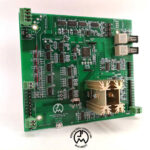
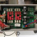
Sequenster is one of the oldest Projects I have developed and the first listed on the projects page because unfortunately for earlier ones I have lost or not documented at all the development process. Sequenster is a step sequencing device, a hardware tool that divides a measure of music into a pre-determined number of note values called “steps.” Furthermore, each step can be configured one way or another, in this device being only possible to let pass or cut the audio signal from the source to the load. Even if today’s step sequencing devices are predominantly software tools, they originally were pure hardware ones, exactly what Sequenster tried to replicate.
sequenster
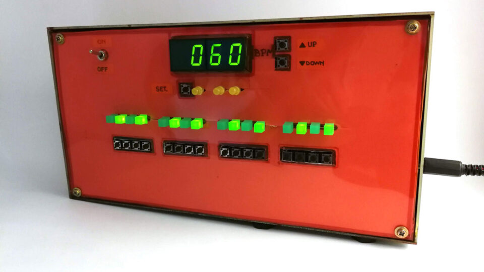
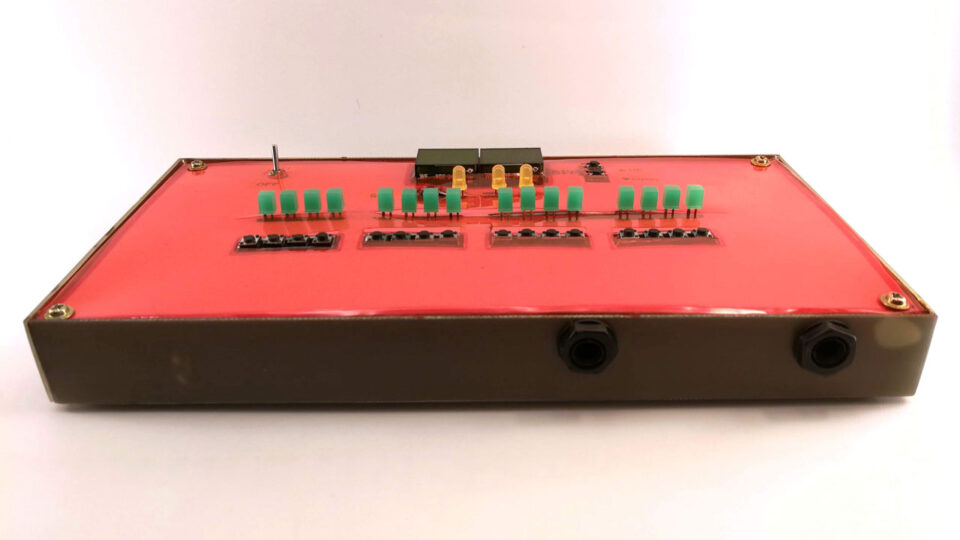
You can observe in Figure 1 a general view of the Sequenster device with an external +5V power jack on the right margin, two 6.3mm audio female connectors on the bottom margin, and the human-machine interface on the front-facing red pannel. Notice a 3-digits seven-segment display used to set the BPM (beats per minute) of the audio signal and 16 green squared LEDs each with a toggle button used to turn on or off a step of the segmented signal.
Hardware Design
The operation of this device is simple and straightforward: the user sets up a BPM using the SET button to select the corresponding digit and the UP and DOWN ones to increase or decrease its value. The BPM is software limited between 60 and 480 beats per minute. The device is only optimized for 1/4 notes, so the duration of a quarter note is extracted from the BPM value as BPM divided by 4. Let’s take for example a tempo of 240BPM which results in a duration of 1000ms for a single note. Furthermore, this duration is divided into 16 steps of 62.5ms, each of them being controlled by toggling the button below its corresponding green LED.
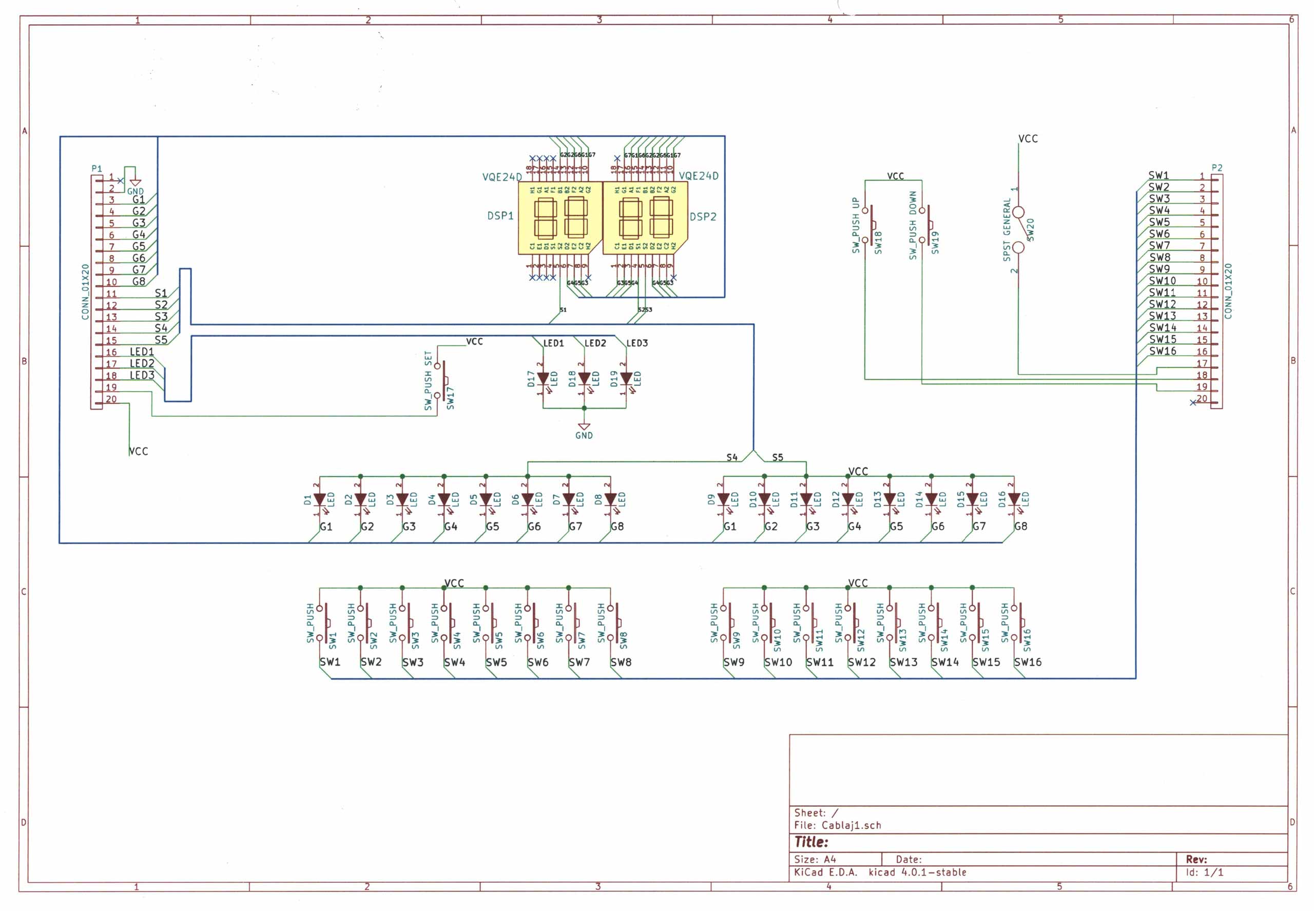
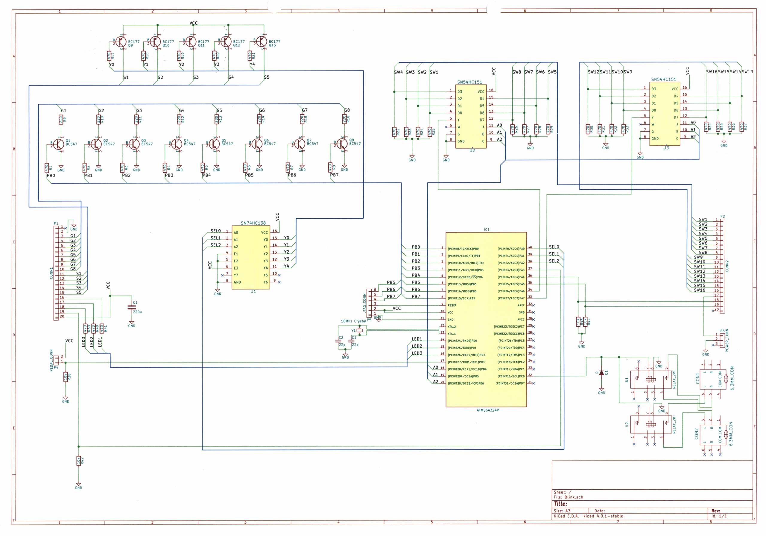
The hardware for this project was organized in two different circuit boards, one with all the human-machine interface devices (LEDs, seven-segment digits, and buttons) whose electric schematic is displayed in Figure 2, and one with the ATMEGA324P microcontroller and other components with the electric schematic displayed in Figure 3.
As far as the LEDs were concerned, I organized them in a multiplexed scheme of 5 rows and 8 columns, 3 rows for the seven-segment digits, and 2 for the 16 green LEDs. The columns had a common cathode controlled with PNP transistors and the rows a common anode controlled with NPN transistors. Because I wanted to reduce the number of IO ports occupied at the microcontroller I used an SN74HC138 3-Line To 8-Line Decoder to control all the PNP transistors. Also, for reading the 16 toggle buttons I used 2 SN74HC151 8-Line To 1-Line Data Selectors. Truth be told, I could probably read and write all the signals without using decoders and selectors but I opted for this solution since I was eager to use these circuits in a real project.
PCB Fabrication and Assembly
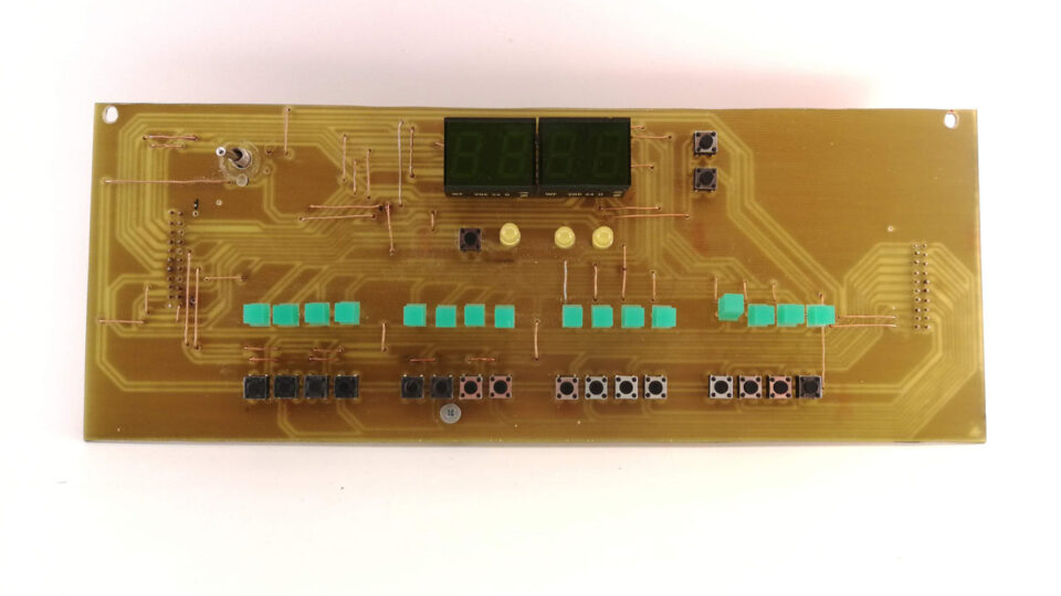
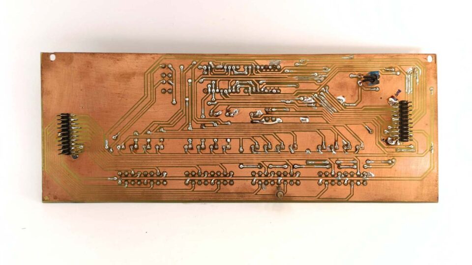
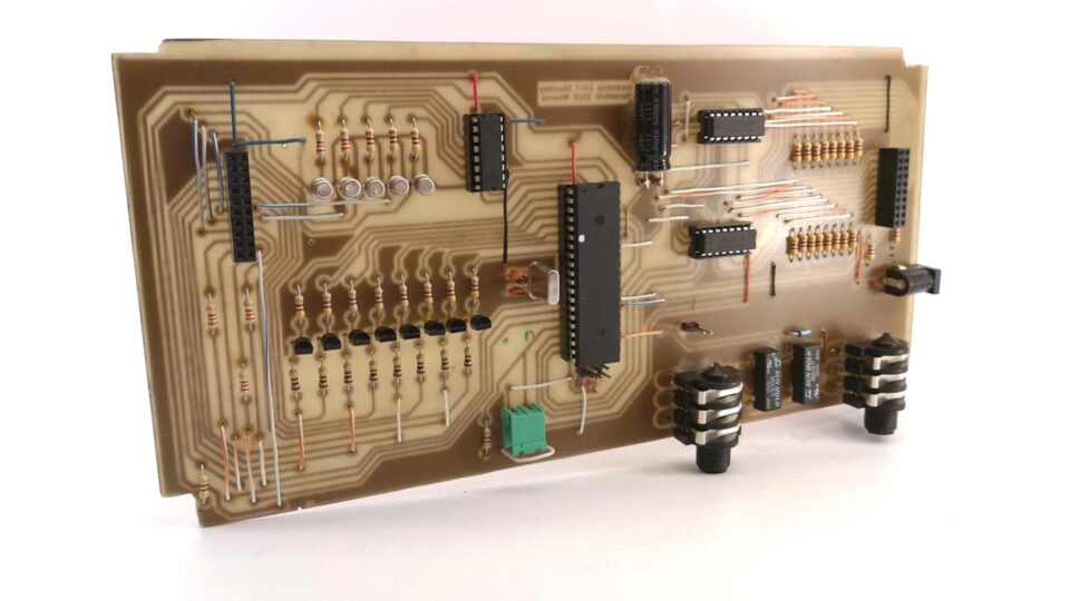
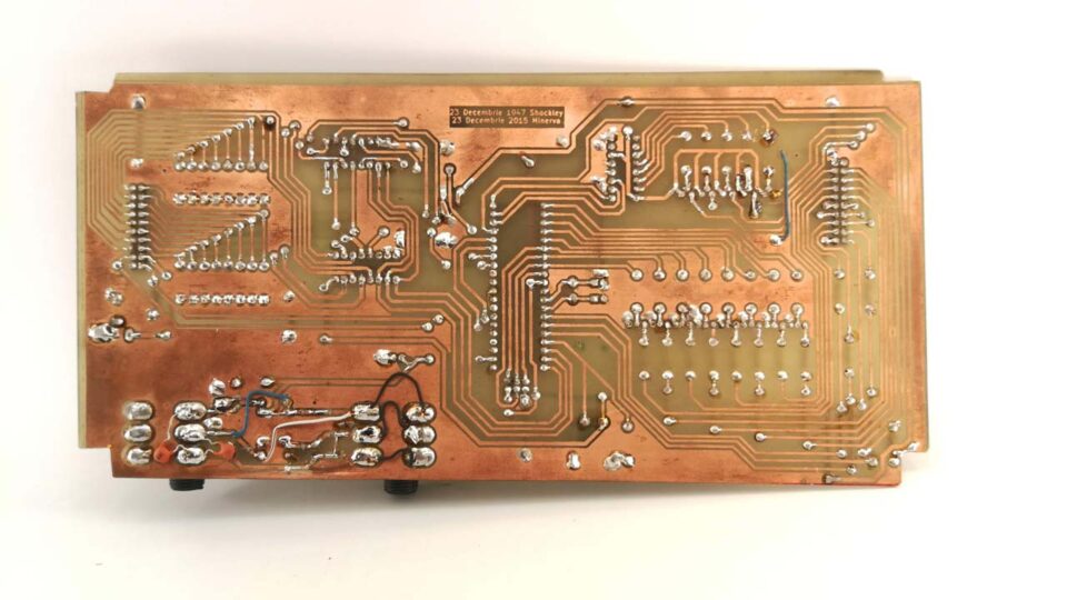
Displayed in Figure 4 and Figure 5 is the first circuit board, the one interfacing the device with the user by LEDs, buttons, and seven-segment digits, and in Figure 6 and Figure 7 is the one including all the electronic components, microcontroller, decoders, data selectors, NPN and PNP transistors. I fabricated both boards in my Workspace using Press’n’Peel foil and ferric chloride for etching.
Final Product
You can view in Figure 8 the final product for which I crafted an enclosure using nothing else than single-sided FR4 substrate boards cut in the corresponding dimensions and soldered on the inside. Looking back I can now say that it was a rudimentary method I had to use in the lack of any other knowledge in 3D Design, 3D printing, and Laser Cutting which I had later gained working at Modulab. Later on, I designed and fabricated custom-made enclosures for my projects such as the ones for SMSGate of sigGen 200.
