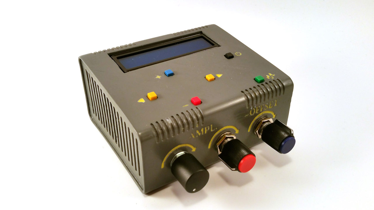
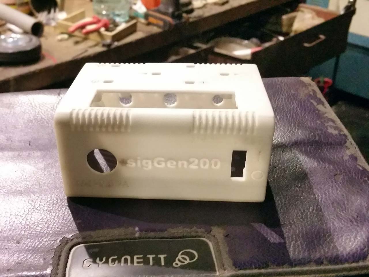
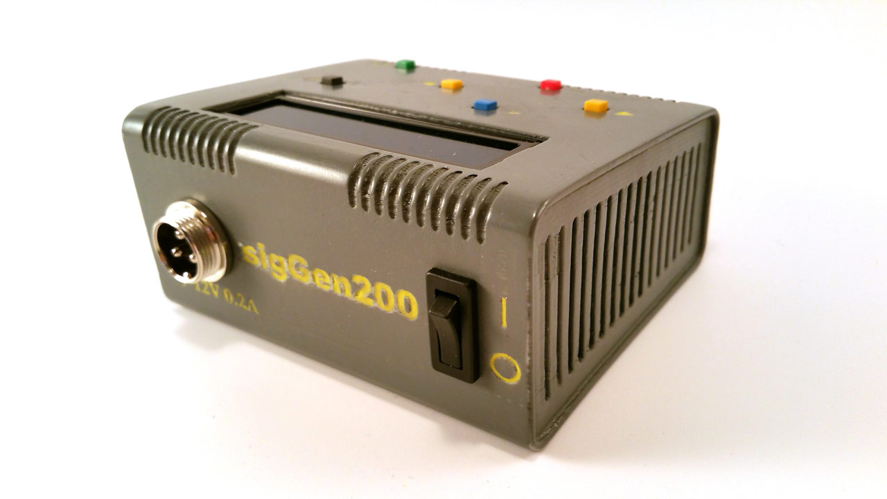
At the beginning of 2017 while I was in the process of arranging my Workspace I began searching for a signal generator to complete my bench tools collection. At that time I only needed a simple entry-level one with frequencies in the couple of kHz range, the kind you would find as a kit on ebay. Since that was a period when I was not missing a single chance of getting my hands into an electronic project, I decided to do it on my own rather than buying it. This is how sigGen 200 (Figure 1) was born, a signal generator with multiple waveforms, variable amplitude and offset and a frequency output up to 200 kHz. This project’s git repository is publicly available here and also the Fusion 360 3D design can be viewed in browser or downloaded here.

Hardware Design
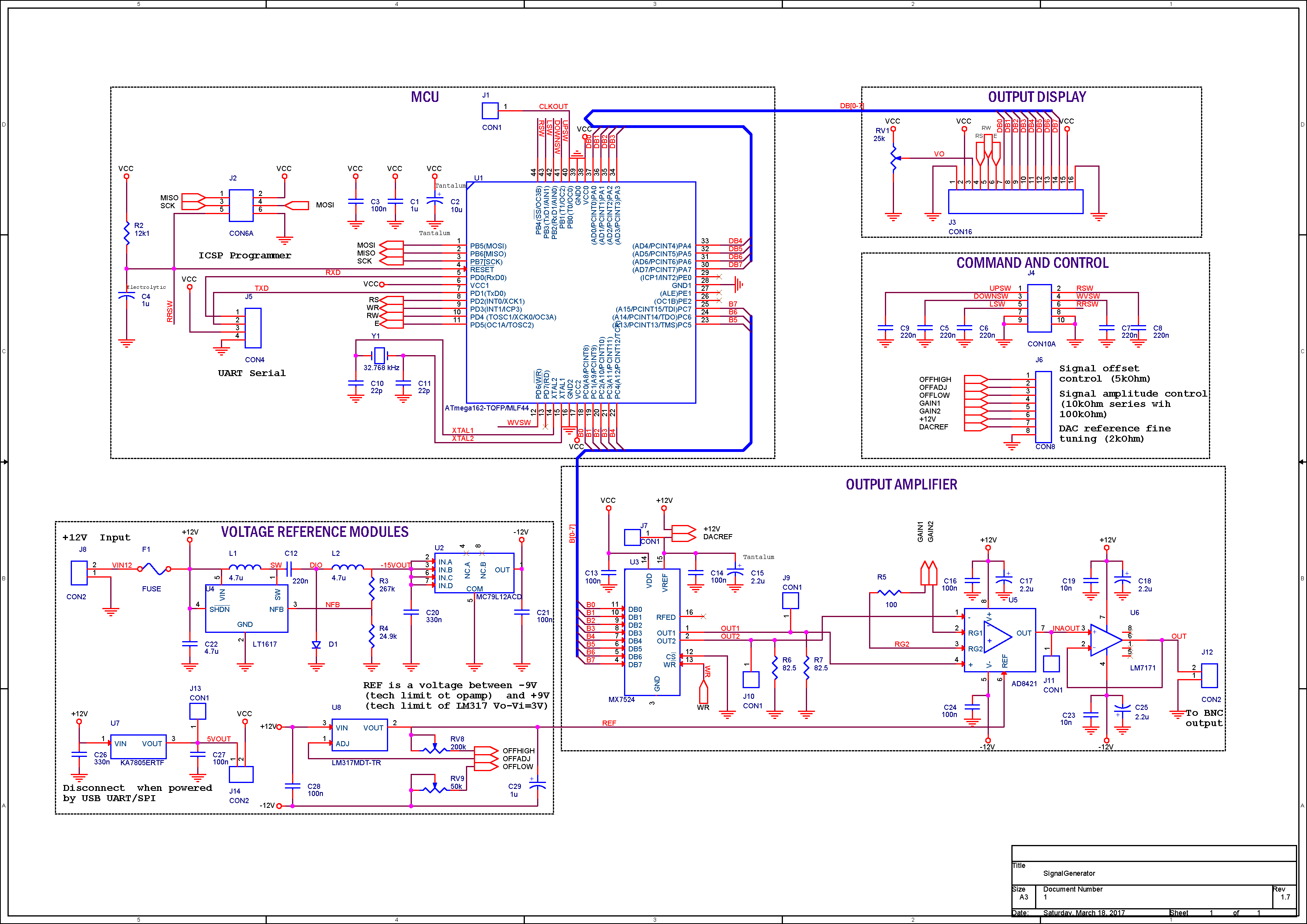
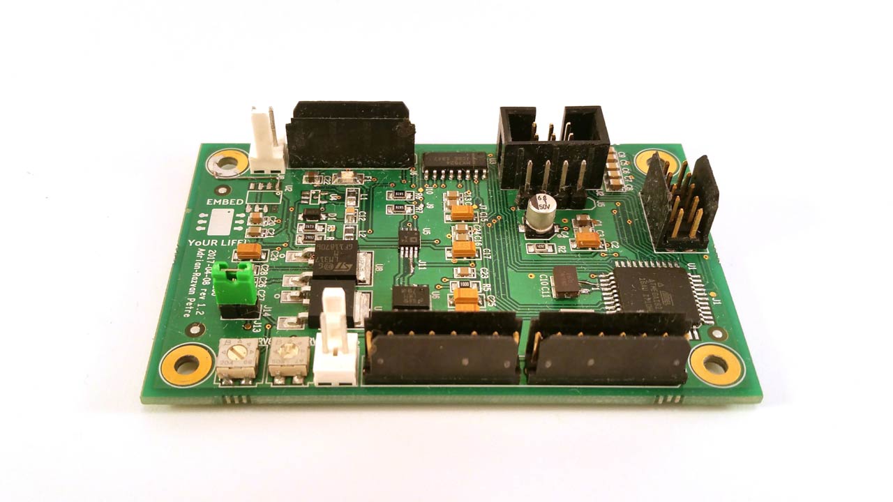
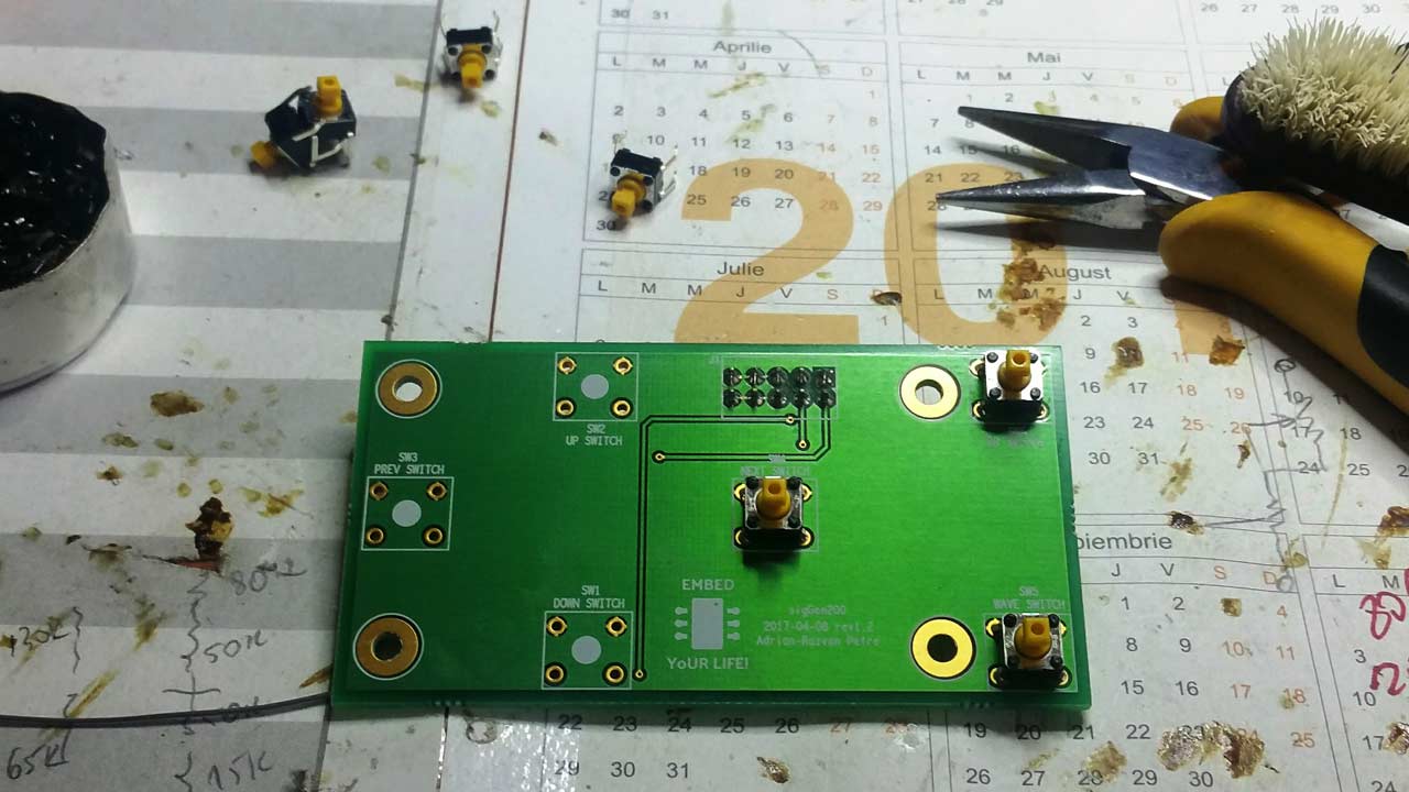
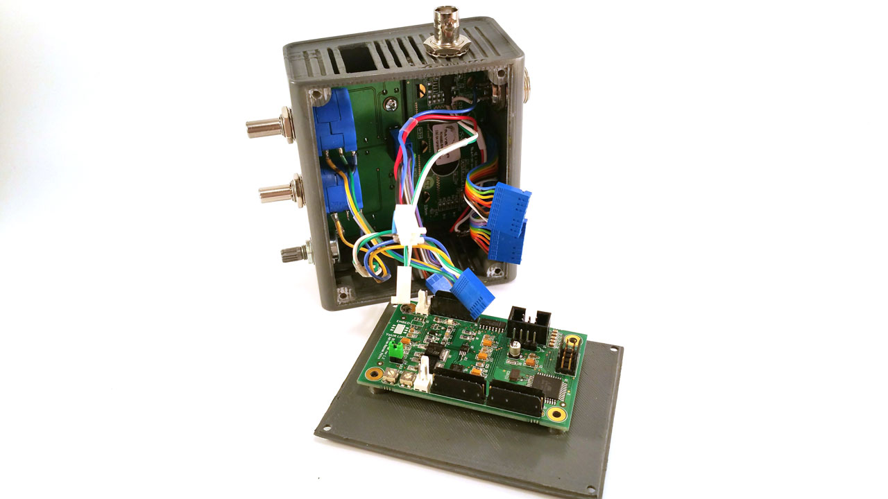
This project was divided in three main circuit boards, MCU, Command and control and Display. The Display one was a 16×2 characters display and the Command and Control just a simple one with 6 switch buttons. However, the MCU one was far more complex with its electrical schematic displayed in Figure 2. Due to the application’s nature, a dual rail supply was required which I thought I could get from a single rail supply by using a LT1617 Micropower Inverting DC/DC Converter. Unfortunately, this circuit was not functional (maybe a failure in soldering or some solder bridge) and I was forced to switch back sigGen 200 design to a dual rail supply. As far as the output signal in regarded, a MX7524 DAC from Maxim Integrated was connected to the Atmega 162 MCU. Finally, an AD8421 Instrumentation Amplifier from Analog Devices was used to increase of decrease the signal’s amplitude.
PCB Assembly
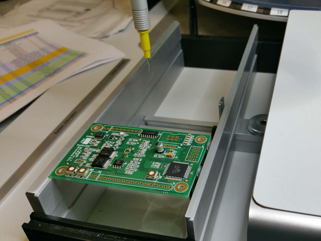
Being also involved in research activities with the Faculty of Electronics from Bucharest gave me access to the facilities of the Faculty’s Center for Electronic Technology and Interconnection Techniques (UPB-CETTI) where solder deposition, reflow oven or vapour phase oven equipment exist. By assembling, soldering and performing rework on projects such as the current one or others like nanodroid, smart cane for VI or SMSGate I learned the basics in Design for Manufacturing (DFM).
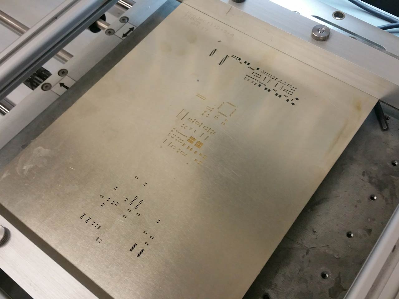
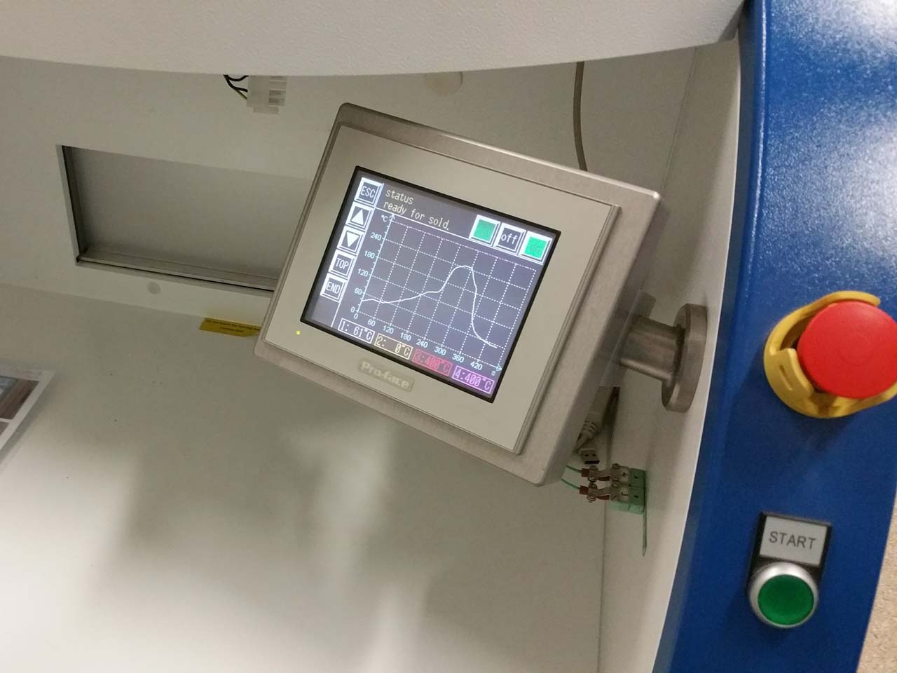
Displayed in Figures 3 to 6 is the MCU board in different stages of assembling. In Figure 3 you can see the board aligned under a solder paste stencil custom-made for this project. After solder paste was deposited, I used a pick and place manual machine to place all the SMT devices and then inserted the board into the vapour phase reflow oven.


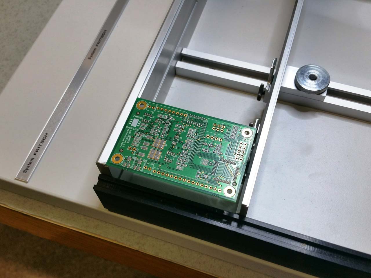
In Figure 7 is displayed the final assembled MCU board (also with THT connectors manually soldered after the reflow process). Notice the MCU in the upper part of the board, voltage regulator in the lower part and connectors disposed all the way near the margins. In Figure 8 is displayed the command and control board including only 6 switches.


Product Design
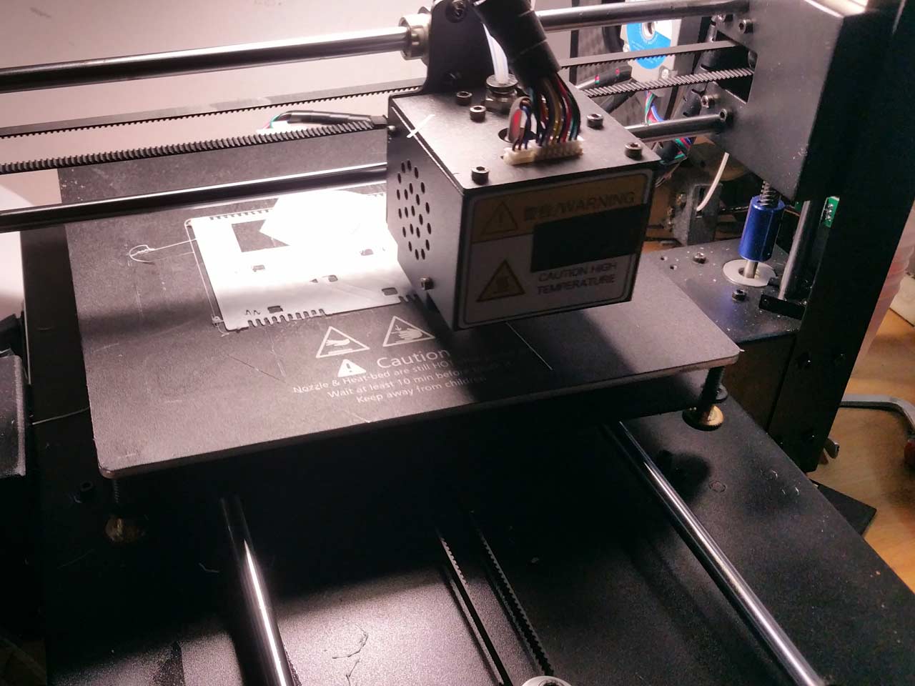
With the experience from previous projects such as Dexter v1 or Dexter v2 and with the Modulab production tools available I developed for sigGen 200 a super detailed 3D printed enclosure, as seen in Figures 9 and 10. The case also included a bottom lid (not present in these figures) which provided access to the electronics inside.


Final Product
In Figures 11 and 12 you can see the final product sigGen 200. Looking back I can now say that it was an interesting and also demanding project enthusiastically designed by someone eager to make his own hardware rather than buying it. It was a project which helped me to gain knowledge in embedded C programming by writing its software in bare-metal C language. Also, I learned a lot about product design by carefully spending many hours crafting its enclosure in Autodesk Fusion 360.


