MicroEDMpulse was a project developed for EDMING SERV CONSULT, a Romanian company that provides automation solutions for, but not limited to, electro-erosion machines. MicroEDMpulse combines the electro-erosion process with ultrasound (US) vibrations. Even if this process is not new, the unique feature of this system is that it matches via an adaptive continuous process the electro-erosion discharge event with a certain time frame from the period of the US wave. In this way, the productivity of the machine is highly increased. Right from the start, I must mention that my contribution to this project was only the redesign of existing electrical schematics and the full development of layout for the corresponding circuit boards, which was also my Master’s Thesis subject. Mr. Gheorghe Jitianu, Managing Director at EDMING SERV CONSULT and Lead Engineer for this project is fully credited for the microEDMpulse idea and has also two patents protecting his invention, RO 131031/2017 and RO 129537/2016.
microEDMpulse (continued)
Hardware Design
The whole microEDMpulse and its functionalities were presented extensively in this previous blog post. I must mention once again that the whole electrical system was designed by EDMING SERV CONSULT and my contribution is only related to the redesign of the three existing PCB modules, the Charging, MCU, and Capacitors ones. The Capacitors module was presented in the previous post about microEDMpulse and in this present one, I only discuss the MCU module.
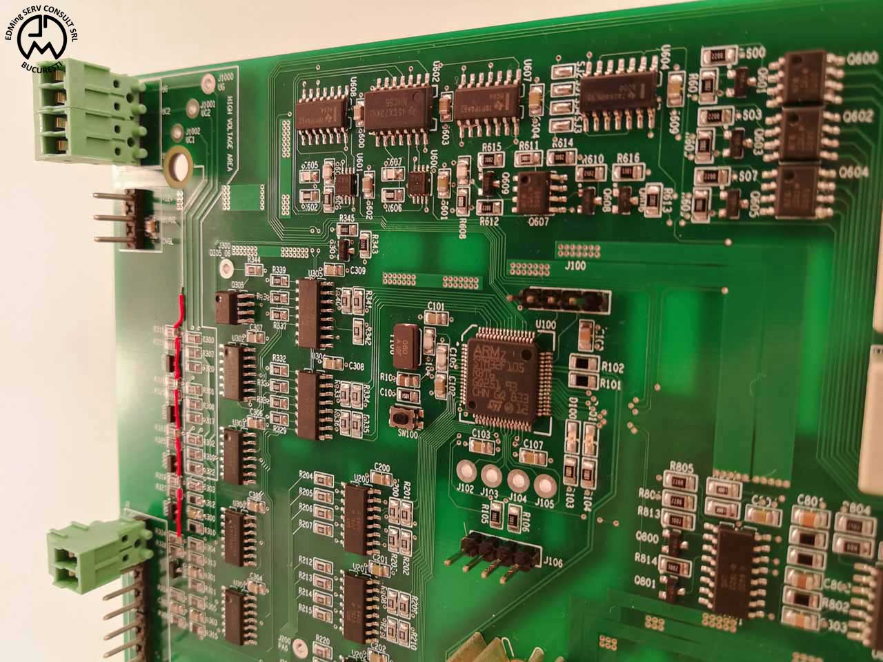
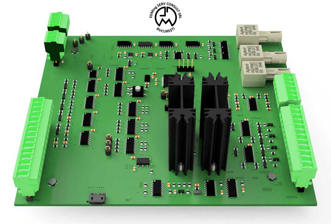
Without disclosing too much of the electrical schematic for this complex circuit board visible in Figure 1, I should say that consisted of an STM32 Arm Cortex microcontroller along with some corresponding peripheric ICs. For the robustness of the system, every input or output of the microcontroller was galvanically separated with optocouplers. You can also notice three optical fiber receiver and transmitters which connect this MCU board with the Capacitors one.
PCB Assembly
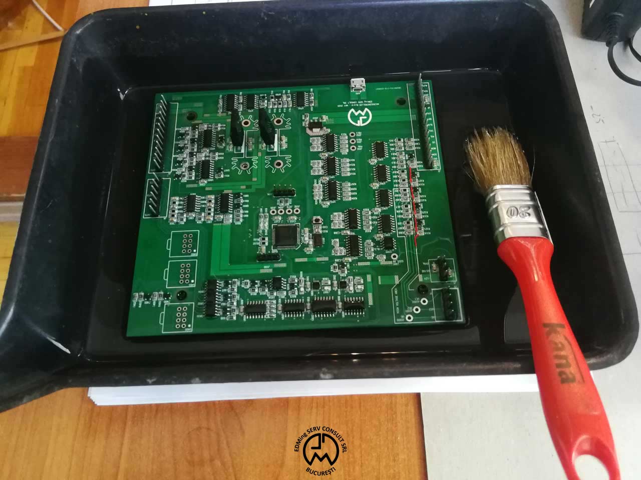
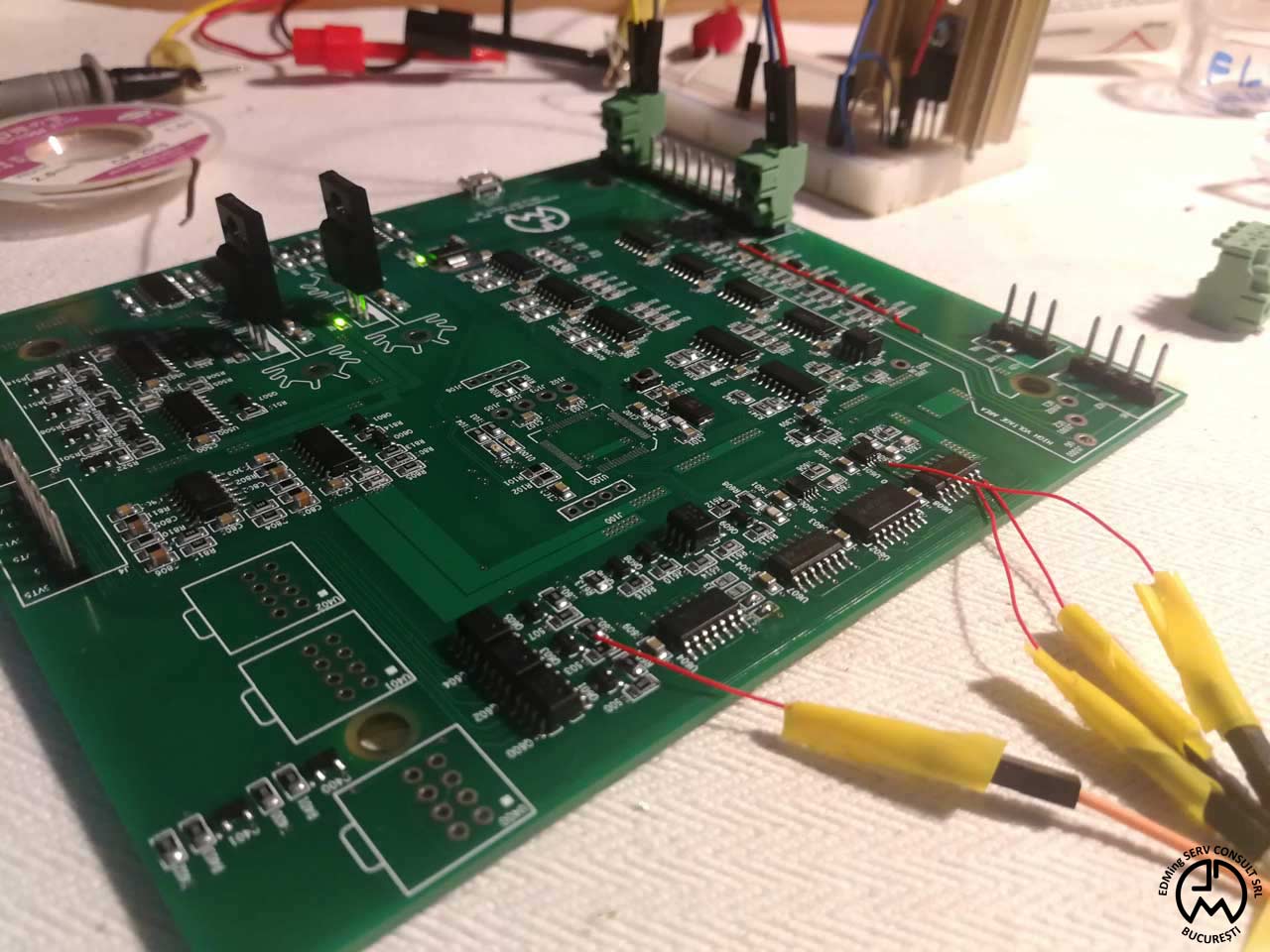
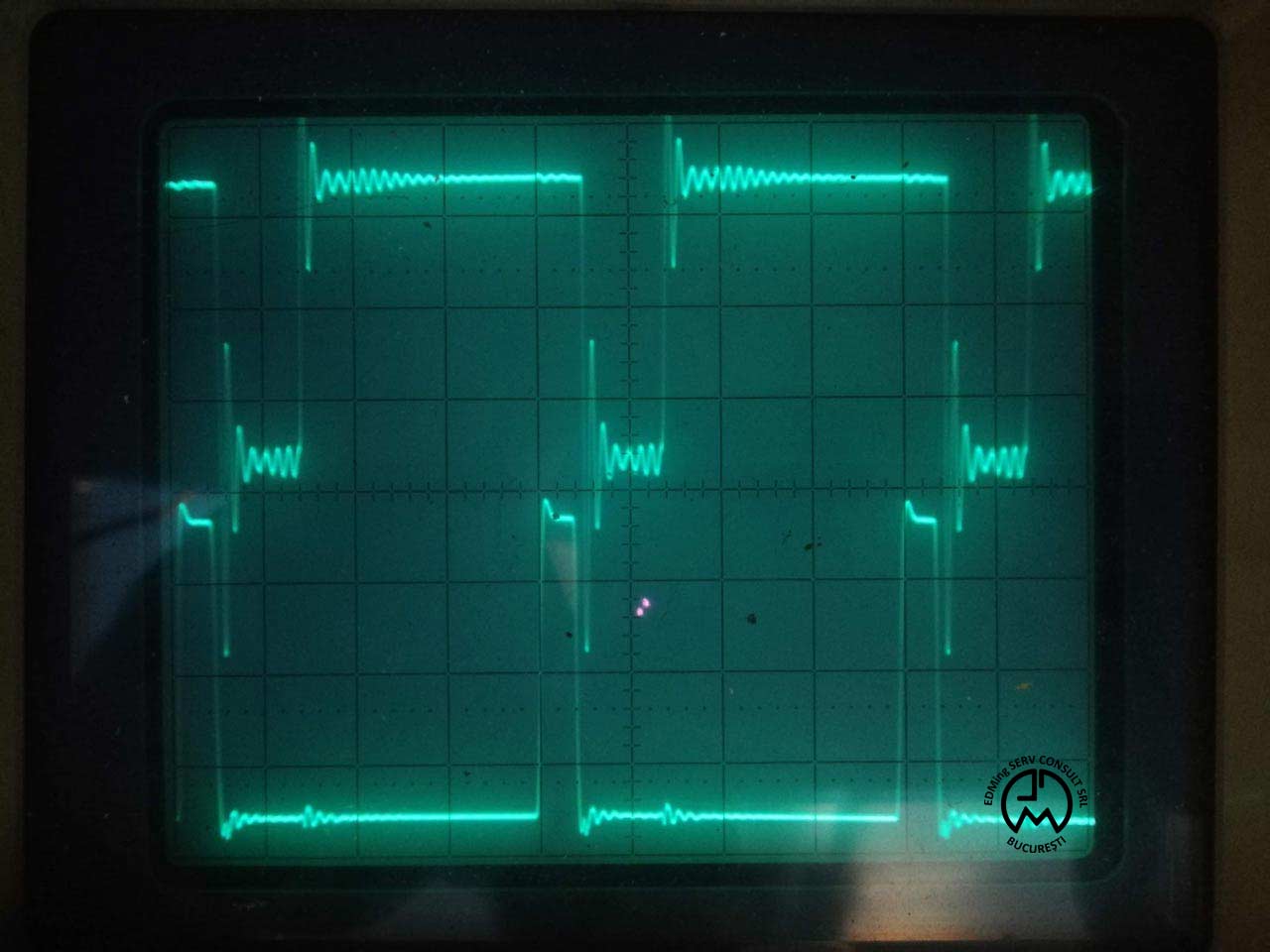
As you can see in Figures 2 and 3 I printed the solder paste, assembled with all the components and reflow soldered this board in the Embeto Electronics Workspace using my custom made DIY reflow oven, reflowster. After the reflow and soldering process was completed, I also tested each functional block of the board using my old HP 1741A oscilloscope as described in Figures 4 and 5 (huge ringing visible in Figure 5, but I was only interested in the timing of the two signals).
Final Product
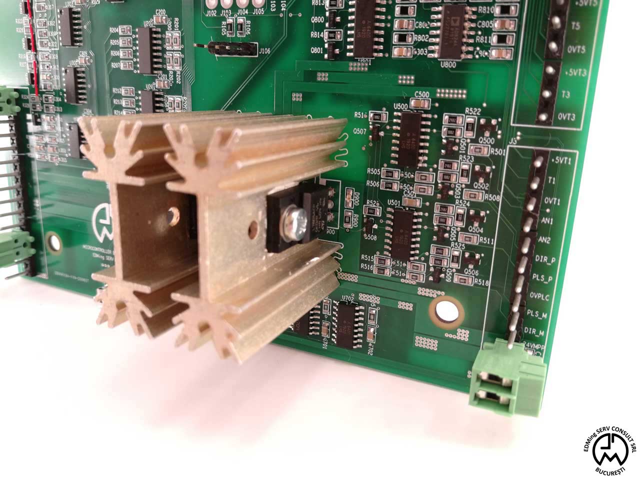
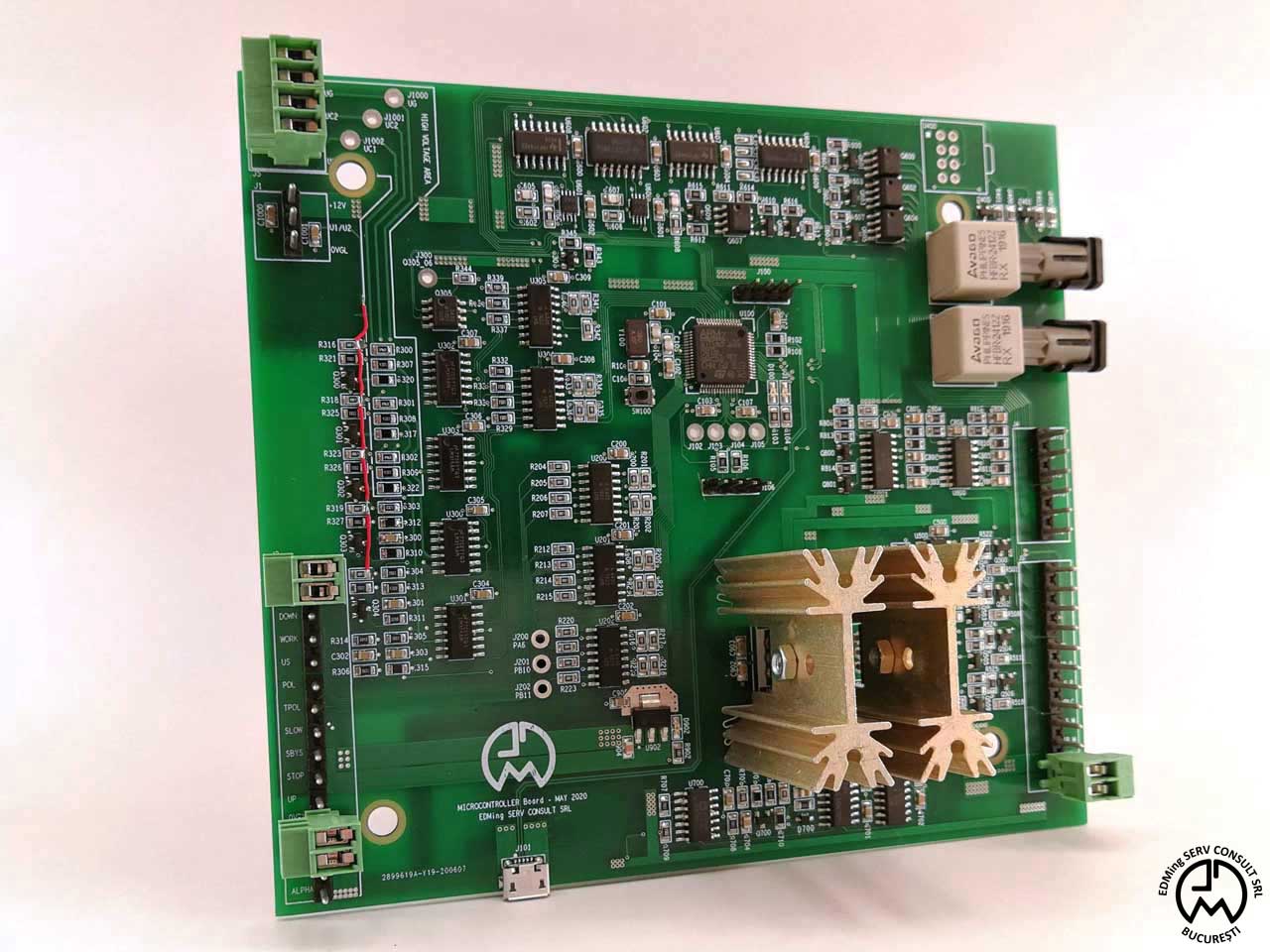
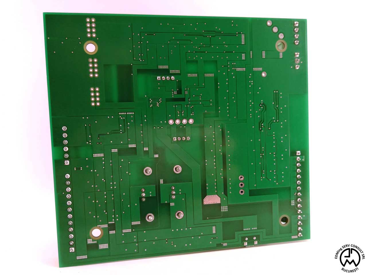
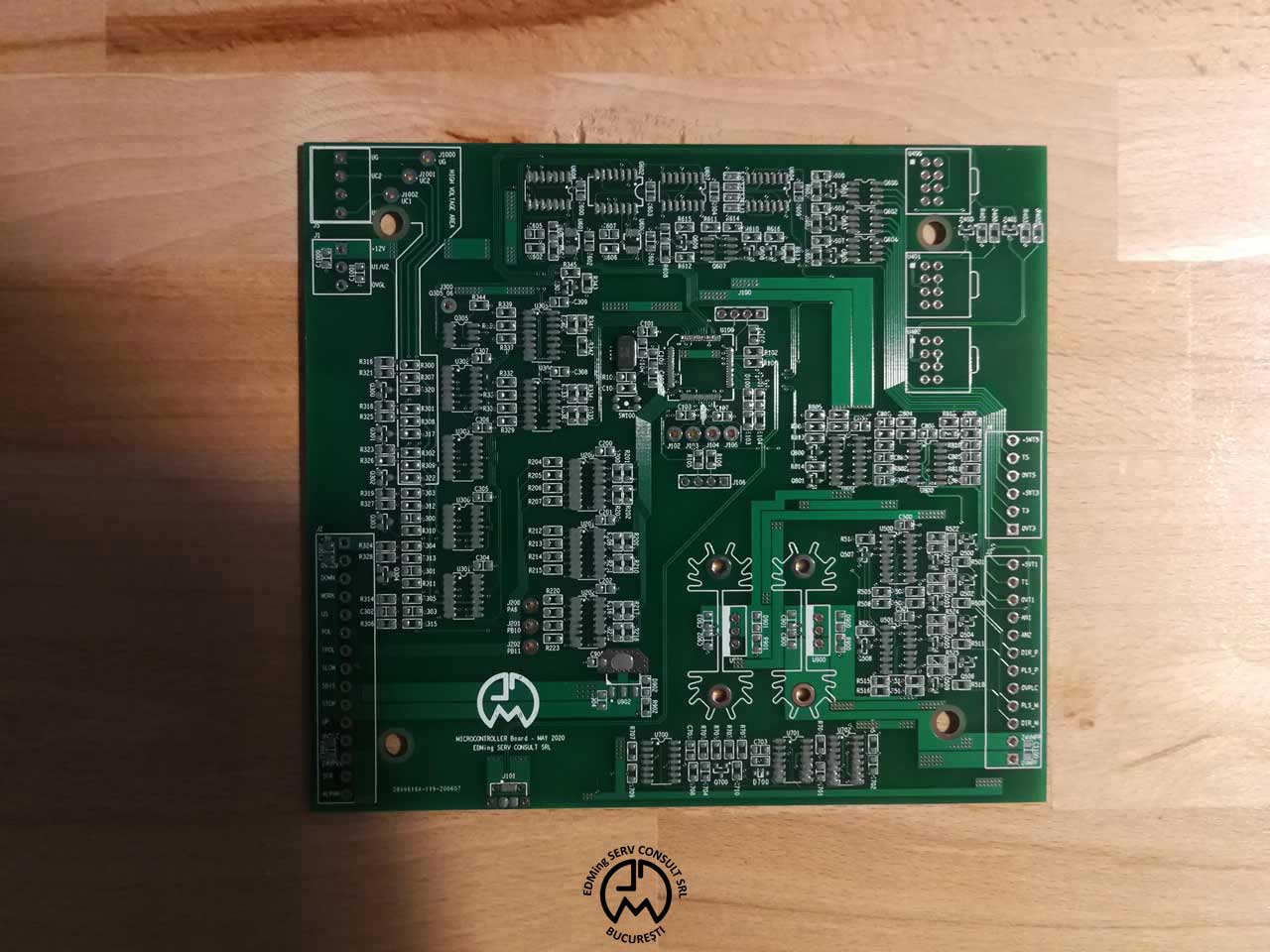
The final MCU board for the microEDMpulse system is visible in Figures 6 and 7 (some red jumper wires attached to the board in Figure 6, due to a small error I committed during the layout design). The initial requirements for this board were the mechanical ones including mounting holes not exactly placed in the extreme corners of the board in order to fit an older existing arrangement from the electrical closet. Another requirement visible from Figures 8 and 9 was to design this module on a two-layers stack-up for debugging purposes, even if two more additional stack-up layers dedicated to power and ground would have been very helpful.